Non-UV Dicing Tapes Market Size
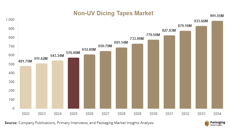
The non-UV dicing tape market size is projected at USD 612.8 million in 2026 and is expected to hit USD 988.6 million by 2034 with a CAGR of 6.2%. The report provides a comprehensive analysis of production capacity, pricing trends, raw material availability, technological developments, the competitive landscape, and regional demand. It further evaluates industry performance through detailed segmentation by type, application, and geography while assessing manufacturing capabilities and investment opportunities.
Non-UV dicing tapes are specialty adhesive tapes designed to securely hold semiconductor wafers during precision dicing operations without requiring ultraviolet irradiation for adhesive release. Global production exceeded 3.45 billion square meters in 2025, while semiconductor wafer dicing applications accounted for approximately 71% of total consumption. MEMS devices contributed nearly 17%, and LED manufacturing represented around 12% of industry demand. Adoption across advanced semiconductor fabrication facilities surpassed 76%, reinforcing the expansion of the non-UV dicing tape market.
Explore more data points, trends and opportunities Download Free Sample Report
Non-UV Dicing Tapes Trends
Increasing Adoption of Advanced Semiconductor Packaging Materials
Semiconductor manufacturers are investing in precision dicing materials capable of supporting thinner wafers and advanced chip packaging. More than 2.4 billion square meters of high-performance non-UV dicing tapes were produced in 2025, accounting for approximately 69% of total output. Ultra-thin wafer processing increased by 18%, while advanced packaging technologies recorded adoption exceeding 41%. These developments continue strengthening the non-UV dicing tape market.
Automation, precision coating technologies, and high-performance acrylic adhesives are improving manufacturing efficiency and product consistency. Automated tape coating lines enhanced production efficiency by approximately 16%, while semiconductor production capacity expanded by 11% globally. Demand from power semiconductor and automotive electronics manufacturing increased by nearly 14%, supporting continuous innovation across the non-UV dicing tape market.
Non-UV Dicing Tapes Market Drivers
Growing Semiconductor Manufacturing Capacity
Global semiconductor sales exceeded USD 650 billion during 2025, while wafer fabrication capacity increased by approximately 9%. More than 37 million wafers were processed monthly worldwide, and advanced chip packaging demand expanded by 15%. Rising investments in semiconductor fabrication facilities continue accelerating the non-UV dicing tapes market.
Non-UV Dicing Tapes Market Restraints
High Manufacturing Costs and Raw Material Price Volatility
Specialty adhesive resins, PET films, and precision coating materials experienced price fluctuations of nearly 12% during 2025. Manufacturing costs increased by approximately 8%, while energy and logistics expenses rose by 7%. These factors reduce profit margins for manufacturers and restrain the non-UV dicing tape market growth.
Non-UV Dicing Tapes Market Opportunities
Expansion of Automotive Electronics and AI Chip Production
Automotive semiconductor production increased by approximately 19%, while AI processor manufacturing expanded by nearly 24% during 2025. Investments in advanced packaging facilities exceeded USD 18 billion, creating significant opportunities for precision dicing materials. These developments generate long-term opportunities across the non-UV dicing tape market.
Challenges in the Non-UV Dicing Tapes Market
Maintaining Precision for Ultra-Thin Wafer Processing
Manufacturers must ensure consistent adhesion, residue-free removal, and dimensional stability for wafers below 50 microns. Quality inspection requirements increased by 21%, while rejection rates for high-precision semiconductor materials must remain below 1%. Continuous R&D investments representing approximately 7% of annual revenue create operational challenges within the non-UV dicing tape market.
Report Scope
| Report Metric | Details |
|---|---|
| Market Size in 2025 | USD 576.9 Million |
| Market Size in 2026 | USD 612.8 Million |
| Market Size in 2034 | USD 988.6 Million |
| CAGR | 6.2% (2026-2034) |
| Base Year for Estimation | 2025 |
| Historical Data | 2022-2024 |
| Forecast Period | 2026-2034 |
| Report Coverage | Revenue Forecast, Competitive Landscape, Supply Chain Disruption, Growth Factors, Environment & Regulatory Landscape and Trends |
| Geographies Covered | North America, Europe, APAC, Middle East and Africa, LATAM |
| Countries Covered | U.S., Canada, U.K., Germany, France, Spain, Italy, Russia, Nordic, Benelux, Rest of Europe, China, South Korea, Japan, India, Australia, Singapore, Taiwan, South East Asia, Rest of Asia-Pacific, UAE, Turkey, Saudi Arabia, South Africa, Egypt, Nigeria, Rest of MEA, Brazil, Mexico, Argentina, Chile, Colombia, Rest of LATAM |
Explore more data points, trends and opportunities Download Free Sample Report
Non-UV Dicing Tapes Market Segmentation
The market is segmented by type and application, with polyolefin-based non-UV dicing tapes accounting for approximately 49% of market revenue, while semiconductor wafer dicing contributes nearly 71% of total industry demand owing to extensive semiconductor manufacturing activities.
Non-UV Dicing Tapes Regional Outlook
North America
North America accounted for approximately 22% of global demand, with annual production exceeding 760 million square meters. The United States represented nearly 84% of regional semiconductor manufacturing demand, supported by investments in advanced semiconductor fabrication and packaging facilities.
Europe
Europe contributed approximately 20% of the market, producing more than 690 million square meters annually. Germany, France, Italy, and the Netherlands generated nearly 68% of regional demand, driven by automotive electronics and industrial semiconductor manufacturing.
Asia-Pacific
Asia-Pacific dominated with approximately 52% market share and production exceeding 1.79 billion square meters annually. China, Taiwan, South Korea, and Japan collectively accounted for more than 81% of regional consumption, supported by large-scale semiconductor fabrication, advanced packaging facilities, and electronics manufacturing.
Latin America
Latin America represented around 3% of global demand. Brazil and Mexico contributed approximately 64% of regional semiconductor packaging activity, supported by increasing electronics assembly operations.
Middle East & Africa
The Middle East & Africa accounted for nearly 3% of industry demand. Israel, the UAE, and South Africa contributed over 55% of regional semiconductor-related consumption, supported by technology investments and electronics manufacturing expansion.
By Type
Polyolefin-Based Non-UV Dicing Tapes: Holding approximately 49% market share, production exceeded 1.69 billion square meters annually. These tapes provide excellent flexibility, residue-free removal, stable adhesion, low particle generation, and compatibility with ultra-thin wafer processing in semiconductor manufacturing.
PVC-Based Non-UV Dicing Tapes: Representing nearly 29% of production, annual output surpassed 1.0 billion square meters. PVC-based tapes deliver high dimensional stability, reliable adhesion strength, mechanical durability, and cost-effective performance for standard semiconductor dicing operations.
PET-Based Non-UV Dicing Tapes: Accounting for approximately 22% of industry output, production exceeded 760 million square meters annually. PET-based products offer excellent tensile strength, thermal stability, precision handling, and compatibility with automated semiconductor processing equipment.
By Application
Semiconductor Wafer Dicing: This segment accounted for approximately 71% of total demand, consuming more than 2.45 billion square meters annually. Non-UV dicing tapes provide secure wafer holding, precise die separation, minimal contamination, high process stability, and excellent compatibility with automated dicing systems.
MEMS Devices: Representing approximately 17% of market demand, MEMS manufacturing consumed nearly 590 million square meters during 2025. Applications require precision handling, low contamination, dimensional stability, and controlled adhesive performance for sensitive microelectromechanical devices.
LED Manufacturing: Accounting for around 12% of total consumption, LED manufacturing utilized approximately 410 million square meters annually. These tapes support accurate chip separation, consistent adhesion, reduced particle contamination, and improved production efficiency during LED wafer processing.
Non-UV Dicing Tapes Market Segmentations
Type
- Polyolefin-Based Non-UV Dicing Tapes
- PVC-Based Non-UV Dicing Tapes
- PET-Based Non-UV Dicing Tapes
Application
- Semiconductor Wafer Dicing
- MEMS Devices
- LED Manufacturing
Non-UV Dicing Tapes Regional Outlook
North America
North America accounted for approximately 22% of global demand, with annual production exceeding 760 million square meters. The United States represented nearly 84% of regional semiconductor manufacturing demand, supported by investments in advanced semiconductor fabrication and packaging facilities.
Europe
Europe contributed approximately 20% of the market, producing more than 690 million square meters annually. Germany, France, Italy, and the Netherlands generated nearly 68% of regional demand, driven by automotive electronics and industrial semiconductor manufacturing.
Asia-Pacific
Asia-Pacific dominated with approximately 52% market share and production exceeding 1.79 billion square meters annually. China, Taiwan, South Korea, and Japan collectively accounted for more than 81% of regional consumption, supported by large-scale semiconductor fabrication, advanced packaging facilities, and electronics manufacturing.
Latin America
Latin America represented around 3% of global demand. Brazil and Mexico contributed approximately 64% of regional semiconductor packaging activity, supported by increasing electronics assembly operations.
Middle East & Africa
The Middle East & Africa accounted for nearly 3% of industry demand. Israel, the UAE, and South Africa contributed over 55% of regional semiconductor-related consumption, supported by technology investments and electronics manufacturing expansion.
Top Players In The Non-UV Dicing Tape Market
- Nitto Denko Corporation
- LINTEC Corporation
- Furukawa Electric Co., Ltd.
- Denka Company Limited
- Mitsui Chemicals, Inc.
- AI Technology, Inc.
- Ultron Systems Inc.
- Maxell, Ltd.
- 3M Company
- Tesa SE
- Adwill (LINTEC)
- Sumitomo Bakelite Co., Ltd.
- Furukawa Electric Industrial Tape Solutions
- Henkel AG & Co. KGaA
- Lohmann GmbH & Co. KG
Nitto Denko Corporation Estimated market share: 20–22% Nitto Denko Corporation is a leading supplier of semiconductor processing materials with a comprehensive portfolio of high-performance dicing tapes for advanced wafer manufacturing. The company maintains extensive research capabilities, precision coating technologies, global production facilities, and strong relationships with semiconductor manufacturers. Continuous investment in ultra-thin wafer processing materials, advanced adhesives, and high-reliability electronic materials strengthens its competitive position across the global semiconductor supply chain. LINTEC Corporation Estimated market share: 16–18% LINTEC Corporation maintains a strong presence through specialized adhesive technologies and advanced semiconductor process materials. The company focuses on precision-engineered dicing tapes, automated manufacturing systems, residue-free adhesive formulations, and continuous product innovation. Its diversified manufacturing footprint, robust quality management systems, extensive R&D investments, and long-standing partnerships with semiconductor fabrication companies reinforce its leadership within the global non-UV dicing tape industry.